
DLP NIRscan Nano Optical Bench
The pages up to this point considered the properties and operation of the individual components within a spectrometer system. Here we examine the design and operation of a specific spectrometer system, the DLP NIRScan Nano, to demonstrate how the individual components work together to make a spectroscopic measurement. Figure N.1 shows the optical bench for the Nano which will serve as the reference figure for the remainder of this section. All of the lenses and optical components employ anti-reflection coatings at the operating wavelengths to minimize reflections and maximize throughput.
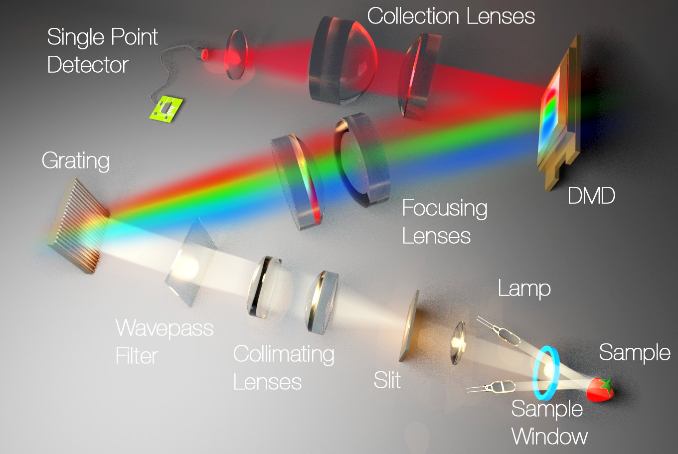
Figure N.1: The optical bench of the DLP NIRScan Nano.
Interrogation Stage: In the specific example shown, two tungsten filament lamps with a lens-shaped output surface illuminate a sample placed against a sapphire sample window. The lamps illuminate the sample at an angle to eliminate specular reflections, which may simply reflect from the surface without absorption, providing no information to the measurement. The sample absorbs a percentage of the NIR light from the lamps and diffusely reflects the remaining light back through the sample window. The interrogation module shown depicts a non-telecentric design since the module does not focus the light prior to delivering the light to the entrance slit. Instead, a single lens collects light from the sample and focuses the light on the slit. Replacing the non-telecentric interrogation stage with a telecentric stage increases the optical power available to the spectrometer and thus increases the SNR. For the design shown, the lenses on the end of the lamps combine with the focusing lens to produce a nominal 2.5 mm –diameter spot on the entrance slit.
The Entrance Slit: The spectrometer comes with a standard entrance slit that is 25 µm in width and 1.69 mm in height. The height of the slit, combined with the magnification of the optical system between the slit and the DMD, determines the height of the slit image on the DMD. In the preferred design, the image height of the slit exceeds the vertical dimension of the DMD’s active area. This choice, along with others discussed later, assist the electronics in detecting misalignments between the slit and DMD positions and the angular orientation of the grating, which provides an electronic means for calibration without physically adjusting any of the components after assembly.
Beyond the entrance slit, two lenses collimate the light from the slit with minimal image distortion and direct the light towards the diffraction grating. A wavelength filter blocks wavelengths below 885 nm to eliminate shorter wavelengths such as visible light entering the slit from room lights or other sources within the spectrometer’s working environment. The periodic ruling of the diffraction grating would direct higher order diffractions of lower wavelengths onto the DMD at the same position as longer wavelengths of interest in the measurement. This overlap would cause the spectrometer to misinterpret the power in the lower wavelengths as part of the power in the higher wavelengths, adding noise and thus error to the measurement process.
The Diffraction Grating: The diffraction grating separates the wavelengths by directing them into different diffraction angles. The choice of groove density for the diffraction grating determines the range of wavelengths imaged onto the active surface of the DMD. The grating efficiently diffracts wavelengths between 900 nm and 1700 nm in wavelength. The two focusing lenses placed after the diffraction grating control the magnification of the slit image on the DMD and the linear dispersion present at the DMD plane. To aid the automatic alignment process mentioned previously, the optical system underfills the DMD in the horizontal direction, such that the spectral range of the light falls on approximately the middle 80% of the DMD. The on-axis design of the optical path reduces image distortions that may arise from the lenses.
Other aspects of the optical system also affect the formation of the slit’s image on the DMD plane. The lenses in the optical system typically provide a magnification of approximately 1.0 for the slit image, as the optimal balance between system resolution and optical power throughput typically occurs at or near this value. The oblique rays from the upper and lower parts of the slit (away from the central axis) experience distortion upon passing through the lenses and diffraction grating, resulting in a curved image on the DMD plane. The curved nature of the image drives the methodologies used to accurately extract the power spectrum of the light from the data collected by the detector.
The DMD:
The standard design for the Nano comes with a DLP2010NIR DMD. The DMD contains 854 columns by 480 rows of aluminum-coated mirrors on a 5.4 μm pitch. The mirrors tilt between +17° and -17˚ for the on and off states, respectively. The angle of the DMD with respect to the incoming light ensures that the on-state mirrors reflect light toward the detector for collection. Assuming that the grating fills 80% of the DMD’s width, this provides an effective linear dispersion of approximately 0.217 nm/μm, with about 1.2 nm of wavelength subtended by each mirror. Installing higher density DMDs in the Nano can improve the resolution at the DMD. Light blocks trap light scattered by mirrors in the off state to reduce noise interference at the detector.
In practice, the DLP board that drives the DMD implements a scanning process for both calibration and measurement purposes. For calibration, a source with known spectral content illuminates the input of the spectrometer. Ideally, the light for a given wavelength images in a vertical line on the DMD. Distortions introduced by the optical system, such as the image bending by the grating mentioned above or misalignment of the optical components, cause the wavelength lines to tilt and/or bend on the DMD. The DLP board implements a scanning process to identify the distortions in the wavelength lines. By identifying these distortions, the DLP can adjust the data processing and scanning algorithms to compensate for the distortions and produce accurate output data on the spectral content of the light. For example, the DLP can scan small rectangles of activated mirrors across the width of the DMD, repeating the scan for rectangles located at different vertical displacements from the center of the DMD. For a known calibration source, the scans provide data on how the optical system maps the wavelengths onto the DMD. Upon completing the calibration process, the spectrometer stores the mapping to use for analyzing data from samples to assist the measurement process. The user can program additional algorithms into the DLP to execute custom scans when performing measurements for specific applications.
The Detector:
A series of lenses collects the light from the DMD and directs the light to an InGaAs point detector. The lens design ensures that the data containing light from the DMD falls on the active area of the detector and minimizes the amount of stray light that falls on the detector area. The detector used in the Nano balances the need for high responsivity at the target wavelengths, sufficient collection area to maximize throughput, and low noise operation. An optional TEC system cools the detector to reduce the noise contributions further. The detectivity (D*) of the detector depends strongly on wavelength. The subsequent processing algorithms must account for this wavelength dependence to produce an accurate representation of the spectrum.
Additional electronics convert and digitize the signal from the detector. A transimpedance amplifier (TIA) converts the photocurrent from the detector into a voltage signal and provides signal amplification. For sampling rates of less than 100 kHz, the TIA operates in photovoltaic mode which provides the operating condition with the lowest amplifier noise. Using a sufficiently high bandwidth for the amplifier ensures that the signal will fully settle before the analog-to-digital converter (ADC) samples the signal. After sampling, the data travels to the on-board microprocessor for processing and analysis.
Extending the integration time of a reading and averaging data over several readings can result in higher signal power and noise reduction, respectively, which increases the SNR of the spectrometer. The electronics of the spectrometer provide the timing and control signals to implement both of these processes if selected by the user.